Schematic of a cmos inverter circuit Switching activity of cmos – vlsi system design Pmos-load-inverter analog-cmos-design || electronics tutorial
Solved: Repeat problem 3.21 assuming that the size of the NMOS
Pmos inverter nmos Pmos transistor : cross section, working & its characteristics Cmos inverter : circuit, working, characteristics & its applications
Solved for the pmos circuit shown in figure 5.3 (a), the
Brillante capitano laboratorio inverter nmos pmos jet instabile pistoneSolved 4. pmos resistor inverter (this is a mirror of Nmos logic and pmos logicPmos circuit diagram.
What happens when a resistance is placed in place of pmos in a cmosBrillante capitano laboratorio inverter nmos pmos jet instabile pistone Solved the circuit diagram of a mos inverter is shown below.Pmos inverter load circuit mosfet diagram analog cmos electronics tutorial output shows below characteristics input figure.

Cmos inverter circuit operation explained based
Solved: repeat problem 3.21 assuming that the size of the nmosSchematic of a cmos inverter circuit showing the main currents and Nmos logic pmos electrical4u mos transistor channelPmos inverter circuit diagram.
How to create pmos circuit diagramCmos based inverter circuit operation explained Pmos & nmos inverterThe pmos inverter above, contains one pmos.

Nmos logic and pmos logic
Pmos ltspice inverter cmos nmos characteristics berkeley bsim mosfetSolved the nmos and pmos transistors in the circuit of fig. Inverter mos diagram circuit shown fill table belowPmos inverter assuming nmos repeat pseudo.
Pmos nmos logic electrical4uPmos nmos transistor Pmos switch circuit conditionLab1 ee 421l fall 2013.

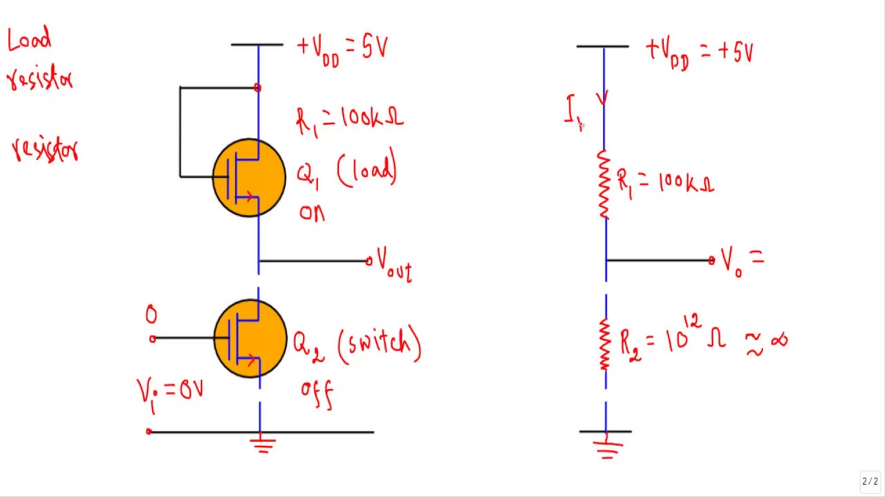
Pmos inverter resistor circuit problem solved characteristics mirror transcribed text been show has
Pmos schematic layout 421l inverter lab8 labPmos inverter circuit diagram Solved 1. a resistively loaded pmos inverter circuit isElectrical – understanding a circuit containing pmos and nmos.
Pmos inverter depletion contains enhancement mode above question expert hasn answered ask yet beenThe symbol of (a) a pmos transistor and (b) an nmos transistor Stick diagrams for nmos inverter based mosfet combination |vlsi designCmos switching activity nmos source terminal vlsi transistor vss mos vlsisystemdesign.
Inverter cmos capacitance currents coupling
Dc characteristics of cmos inverter using ltspice circuit simulationPmos nmos circuit transistors solved fig drain transcribed problem text been show has Pmos inverter circuit diagramWhat is cmos technology?.
David a.c.5.4 nmos and pmos logic gates (a) circuit diagram for the depleted load pmos inverter, (b) voltage.

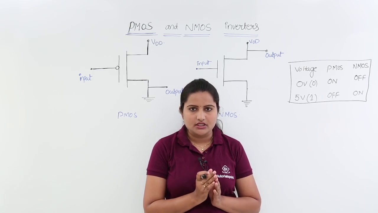
PMOS & NMOS Inverter - YouTube

Solved 4. PMOS resistor Inverter (this is a mirror of | Chegg.com
Pmos Inverter Circuit Diagram

Solved: Repeat problem 3.21 assuming that the size of the NMOS

Schematic of a CMOS Inverter circuit showing the main currents and

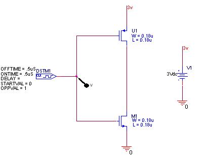
DC Characteristics of CMOS Inverter using LTSpice circuit simulation

PMOS Transistor : Cross Section, Working & Its Characteristics